


























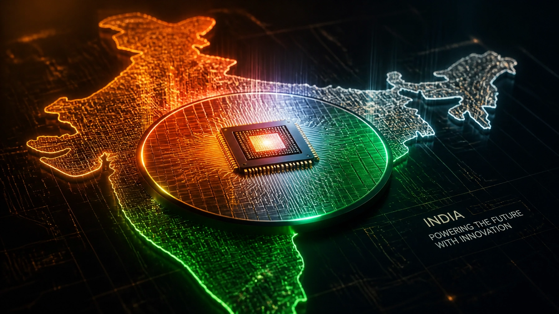

The global technological landscape is undergoing a tectonic shift, and at the heart of this transformation lies the humble silicon chip. For decades, India’s role in the global tech hierarchy was largely defined by its prowess in software services and IT support. However, the dawn of Semiconductor Mission 2.0 signals a departure from this legacy, ushering in an era where India seeks to move from the periphery of hardware consumption to the epicenter of hardware creation.
Announced with a staggering $20 billion strategic outlay, Semiconductor Mission 2.0 is more than just a fiscal package; it is a comprehensive blueprint for deep-tech sovereignty. While its predecessor, ISM 1.0, focused on the Herculean task of establishing massive fabrication plants (fabs), the 2.0 iteration pivots toward a more nuanced, ecosystem-driven approach. This evolution is set to be a massive catalyst for change for the Indian startup ecosystem, redefining how entrepreneurs, investors, and global partners perceive the potential of Indian innovation.
1. The Design-Linked Incentive (DLI) as a Catalyst for Change under Semiconductor Mission 2.0
One of the most profound shifts in this new mission is the elevated priority given to the design ecosystem. In the past, hardware startups in India faced insurmountable barriers to entry, primarily due to the prohibitive costs of Electronic Design Automation (EDA) tools and the lack of access to fabrication facilities. Semiconductor Mission 2.0 addresses these pain points head-on through the revitalized Design Linked Incentive (DLI) scheme.
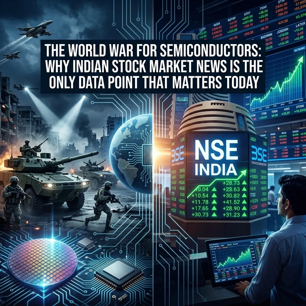
The DLI scheme is designed to democratize access to high-end chip design. By providing financial support and infrastructure for "fabless" companies, the government is essentially subsidizing the intellectual labor required to compete with global giants like Qualcomm and Nvidia. As of 2026, over 24 semiconductor design startups have already been integrated into this framework, attracting approximately ₹430 crore in venture capital. This transition from capacity creation to technological depth ensures that India is not just a factory floor for foreign designs, but a laboratory for indigenous intellectual property.
2. Democratizing Silicon: Lowering Barriers for Fabless Innovators
For an aspiring entrepreneur, the "valley of death" in hardware is significantly deeper than in software. Development cycles are longer, capital requirements are higher, and the risk of failure is absolute. However, the strategic provisions within Semiconductor Mission 2.0 are designed to provide a "soft landing."
By offering access to a shared EDA platform: which has already recorded over 2.25 crore tool hours: the mission allows startups to iterate and prototype without the multi-million dollar overhead typically associated with chip design. This move is reminiscent of how cloud computing revolutionized the software industry; it has turned a massive capital expenditure (CapEx) into a manageable operating expense (OpEx).
This environment has contributed to the start-up flood in India, where deep-tech is finally catching up to the consumer internet boom. Founders are no longer limited to building apps; they are building the very processors that run them.
3. Geopolitical Resilience and the Global Supply Chain
The geopolitical climate has made semiconductor self-reliance a matter of national security. As global powers engage in "chip wars," India’s positioning as a neutral, stable, and high-growth alternative is its greatest value proposition. Semiconductor Mission 2.0 leverages this sentiment to integrate Indian startups into the global supply chain.

By focusing on compound semiconductors and specialty fabs: technologies critical for electric vehicles (EVs), 6G telecom, and green energy: India is targeting high-growth niches where it can establish early dominance. Unlike the cutting-edge 2nm silicon nodes that require billions in investment, these specialty sectors allow Indian startups to achieve exponential growth with relatively leaner operations. This strategic focus ensures that India provides a diversified alternative to the Taiwan-centric supply chain, a move that is highly lauded by international investors and trade partners.
4. Deep Tech Sovereignty: Building the Next Global Titans
The "mission" of Semiconductor Mission 2.0 is not merely to support small businesses but to architect the next generation of global tech titans. The focus is on creating indigenous Intellectual Property (IP). For too long, Indian tech has been "service-heavy" and "IP-light."
The government’s "Chips to Startup" (C2S) program, which involves over 397 universities and startups, is a testament to this commitment. By fostering an environment where 56 chips have already been designed and fabricated at the Semiconductor Laboratory in Mohali, the mission is creating a pipeline of proven technology. This is a critical step because, in the semiconductor world, "provenance" is everything. A startup with a fabricated and tested chip is infinitely more bankable than one with only a digital schematic.
For these startups, proper business management becomes essential as they scale from small design houses to global IP providers. The complexities of international patent law and "legitimate purpose" data-driven insights will require a level of professionalization that matches their technical brilliance.
5. The Human Capital Advantage: Bridging the 2 Million Talent Gap

A mission is only as good as the people executing it. The semiconductor industry currently faces a global talent shortage, with India identifying a gap of approximately 2 million specialists. Semiconductor Mission 2.0 addresses this by integrating workforce development into its core strategy.
The goal is to produce 275,000+ semiconductor specialists by 2030 through curriculum modernization and industry-academia interfaces. This influx of talent will be the primary fuel for the startup engine. As large-scale fabs like those from the Tata Group and Micron become operational, they will act as "anchor institutions," spinning off talent and sub-contracting opportunities to smaller, agile startups. This creates a virtuous cycle of innovation and employment that is essential for a healthy economic rebound.
6. Challenges and the Path Ahead: Avoiding the "Tax-Break Trap"
While the optimism surrounding Semiconductor Mission 2.0 is palpable, the path is fraught with challenges. India has historically struggled with regulatory bottlenecks and inconsistent policy implementation. Furthermore, the government has shown a firm stance against providing unconditional concessions, as seen in its rejection of Elon Musk's calls for tax breaks.
For the semiconductor mission to succeed, it must maintain a balance between aggressive incentives and strict performance milestones. The focus must remain on "value creation" rather than "subsidy seeking." Startups must utilize these resources for high-impact innovation rather than just operational cushioning.

Conclusion
Semiconductor Mission 2.0 represents a transformative leap in India’s industrial policy. By pivoting from a purely manufacturing focus to an IP-centric, design-led strategy, the government is providing Indian startups with the tools to compete on a global stage. The mission is not just about building chips; it is about building a future where "Designed in India" carries the same weight as "Designed in California."
As the first fabs commence commercial production and the DLI-backed startups begin to tape out their first chips, the narrative of the Indian startup ecosystem will fundamentally change. We are moving beyond the era of service delivery and entering the age of deep-tech creation. For the analytical observer, the message is clear: the silicon revolution in India has finally arrived, and it is being led by a new generation of disciplined, innovative, and government-backed entrepreneurs. 🚀
For the latest updates on India's economic landscape and high-profile business moves, stay tuned to Business Tantra.