


Tata Electronics & ASML Inks Pact: What It Means For India’s Chip Ambitions
The global semiconductor landscape is witnessing a tectonic shift as India positions itself as a formidable contender in high-tech manufacturing. In a landmark development for the nation's industrial roadmap, the Tata Electronics & ASML pact has officially been inked, signaling a transformative era for the India Semiconductor Mission. This strategic partnership, finalized between the semiconductor arm of the Tata Group and the Dutch lithography giant ASML, is not merely a commercial transaction; it is a catalyst for change that seeks to democratize advanced chipmaking capabilities on the Indian subcontinent.
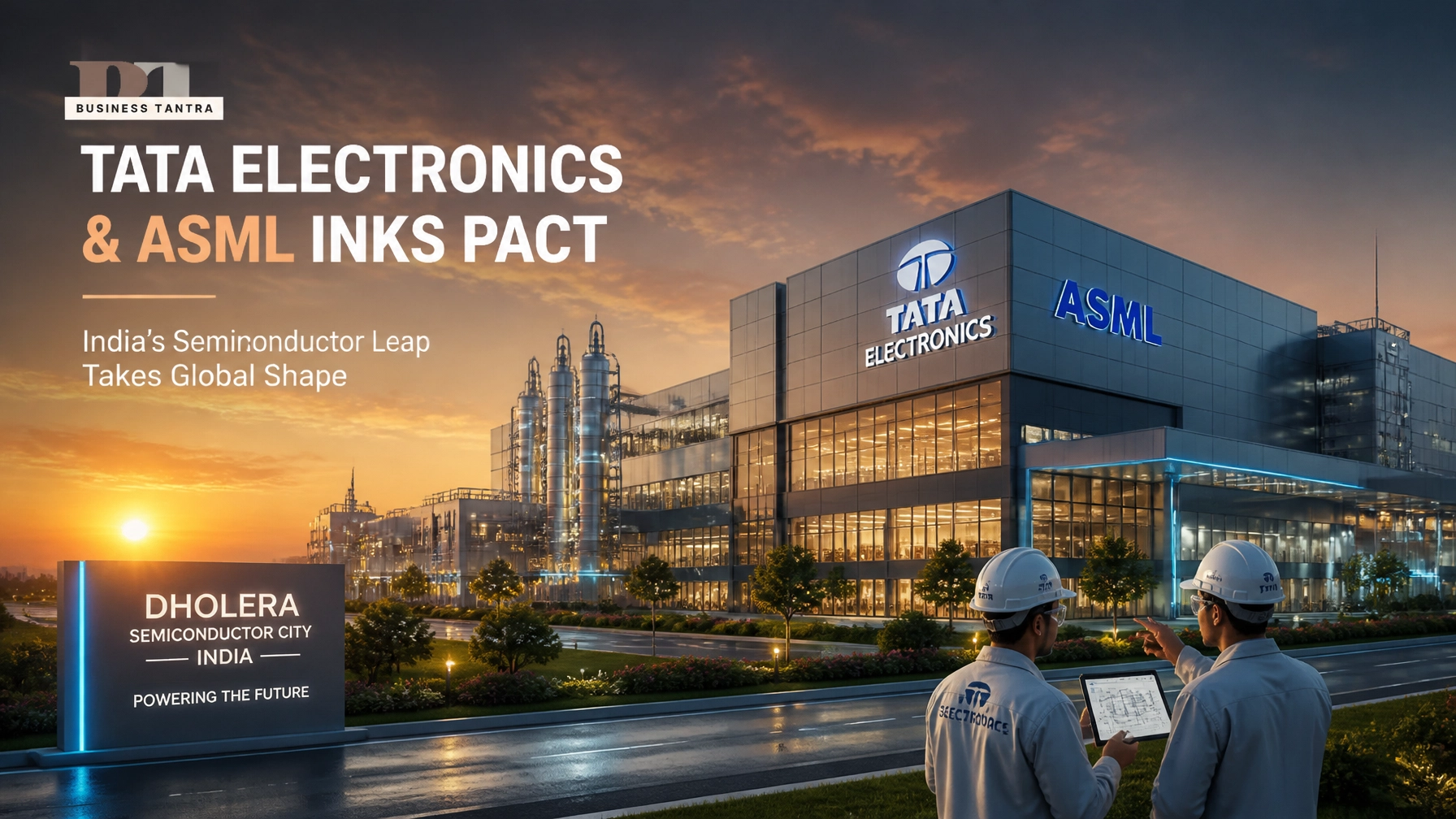
As the world grapples with supply chain vulnerabilities and the rising demand for silicon in everything from automotive systems to artificial intelligence, this agreement stands as a definitive mission statement. By aligning with ASML: the near-monopolist in the world’s most advanced lithography technology: Tata Electronics is securing the precision tools required to power India’s first commercial-scale 300 mm front-end semiconductor fabrication plant in Dholera, Gujarat.
1. The Core of the Partnership: Lithography and the Dholera Fab
At the heart of the Tata Electronics & ASML pact is the deployment of ASML’s holistic suite of advanced lithography solutions. Lithography is the most critical and complex stage of the chip-making process, involving the use of light to "print" microscopic circuit patterns onto silicon wafers. Without the mastery of this process, achieving high yields and commercial viability in a modern "fab" (fabrication plant) is virtually impossible.
The Dholera facility, representational of an $11 billion investment (approximately ₹91,000 crore), is designed to be India’s premier 300 mm wafer plant. Through this partnership, ASML will provide more than just the physical scanners; the deal encompasses a sophisticated layer of software, process control, and technical services. This ensures that as Tata Electronics ramps up production, it can hit the stringent quality and throughput targets demanded by global clients in the automotive, mobile, and IoT sectors.

2. Why ASML is a Catalyst for India’s Chip Ambitions
ASML’s involvement is a significant vote of confidence in India’s business ecosystem. As a linchpin of the global semiconductor supply chain, ASML’s decision to deepen its footprint in India through Tata Electronics suggests a long-term strategic bet.
- Access to Strategic Technology: By securing a direct line to ASML’s Deep Ultraviolet (DUV) lithography systems, India joins an elite group of nations capable of handling 28 nm to 110 nm nodes. While these are not the 3 nm nodes found in the latest smartphones, they are the "workhorse" nodes essential for the global automotive and industrial sectors.
- Operational Excellence: The collaboration extends to the "volume ramp" phase. ASML’s engineers will work alongside Tata’s team to ensure "seamless operations," a critical factor in avoiding the expensive downtime that often plagues new fabs.
- Supply Chain Resilience: This pact revitalizes India’s position in the "China+1" strategy, offering global manufacturers a legitimate alternative for chip sourcing outside of traditional East Asian hubs.
For those tracking the broader latest business stories, this move is being viewed by analysts as the final piece of the puzzle for Tata's semiconductor roadmap, which also includes a major assembly and test facility in Assam.
3. Empowering the India Semiconductor Mission: Talent and Ecosystem
A recurring challenge in the high-tech sector is the "skills gap." The Tata Electronics & ASML pact addresses this head-on through a robust talent development initiative. The agreement outlines joint programs to train Indian engineers and technicians in the intricacies of lithography and fab operations.
Building a sustainable domestic talent pool is a cornerstone of the India Semiconductor Mission. By creating a pipeline from India’s top engineering colleges to the fab floor in Dholera, the partnership ensures that the facility will eventually be run and optimized by local experts. This focus on human capital is designed to produce exponential growth in India’s technical self-reliance, moving the country away from a dependence on expatriate expertise.

4. A Global Strategic Alignment: The India-Netherlands Nexus
The signing of this pact was not merely a corporate event; it carried significant diplomatic weight, attended by the Prime Ministers of both India and the Netherlands. This elevates the semiconductor industry to a core pillar of the India-Netherlands strategic partnership.
The Netherlands, home to ASML and a historic center for maritime trade, is now becoming India's gateway to advanced European technology. This bilateral cooperation provides a data-driven insight into how modern geopolitics is being shaped by silicon. For India, the alliance provides a secure electronic communications network for technology transfer, while for the Netherlands, it opens a massive, rapidly growing market for its most sophisticated exports.
5. Complementary Shifts: The Enterprise AI Push and Student Venture Networks
The Tata Electronics & ASML pact does not exist in a vacuum. It is part of a broader "Enterprise AI Push" currently sweeping the nation. As India’s enterprise AI momentum begins to match global standards, the demand for domestically produced chips will only intensify. Large-scale AI deployment requires massive compute power, and having a local supply of the necessary components: power management ICs and sensors produced at Dholera: will be a game-changer for Indian tech giants.
Simultaneously, initiatives like the ICAN (IA Campus Analyst Network), launched by India Accelerator and Internshala, are cultivating the next generation of tech entrepreneurs. By building a student venture network, India is ensuring that the chips designed and manufactured through the Tata-ASML partnership find a home in innovative local startups.

6. Challenges and the Road Ahead
While the Tata Electronics & ASML pact is a monumental step, the journey to becoming a global semiconductor hub is fraught with operational challenges.
- Infrastructure Reliability: Semiconductor manufacturing requires an uninterrupted supply of ultra-pure water and stable electricity. The Dholera Special Investment Region must meet these world-class standards consistently.
- Yield Management: Achieving high yields on a 300 mm wafer is a feat of engineering that requires years of fine-tuning. The partnership with ASML and Taiwan's PSMC will be put to the test during the initial production runs.
- Global Competition: Other nations, including the US, Germany, and Japan, are also aggressively subsidizing their local chip industries. India must maintain its policy consistency and incentive structures to stay competitive.

Conclusion
The Tata Electronics & ASML pact represents a definitive turning point for the India Semiconductor Mission. By securing the world's most advanced lithography tools and embedding a deep talent-development framework, Tata Electronics is doing more than building a factory; it is architecting an ecosystem.
This partnership serves as a legitimate purpose for India’s entry into the high-stakes world of front-end manufacturing. As the Dholera fab begins its journey toward commercial production, the ripple effects will be felt across the automotive, telecommunications, and AI sectors. For entrepreneurs and investors alike, this is an optimistic signal that India is no longer just a consumer of technology: it is becoming a vital, sovereign producer of the silicon that will define the 21st century.
For more deep dives into the Indian economy and corporate updates, visit our About Us page or browse our latest economics news.